p-n junction
A p–n junction is a boundary or interface between two types of semiconductor material, p-type and n-type, inside a single crystal of semiconductor. It is created by doping, for example by ion implantation, diffusion of dopants, or by epitaxy (growing a layer of crystal doped with one type of dopant on top of a layer of crystal doped with another type of dopant).
If two separate pieces of material were used, this would introduce a grain boundary between the semiconductors that would severely inhibit its utility by scattering the electrons and holes .
The interface at which p-type silicon and n-type silicon make contact with each other.
At this coupling point, free electrons (n-type) and holes (p-type) cancel each other and form a "depletion zone" that acts as a non-conductive barrier. The PN junction is one of the primary building blocks of semiconductors.

Diodes and Thyristors
A diode (one way valve) is a PN junction with p-type on one side and n-type on the other. When a positive voltage is applied to the p-type side (forward bias), it shrinks and overcomes the depletion zone, causing the current to flow from the p-type to the n-type side. When a negative voltage is applied to the p-type of the diode (reverse bias), it increases the depletion zone and prevents current from flowing
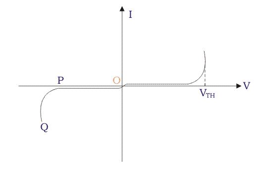
Built like two diodes in a row (three PN junctions) but with a third terminal, a thyristor is a one-way valve that, once turned on, lets current flow until it falls below a certain threshold .
